Registers
The HD44780 has two 8 bit registers, an instruction register (IR) and a data register (DR).
The IR stores instruction codes such as display clear and cursor shift, and address information for display data RAM (DD RAM) and character generator RAM (CG RAM). The IR can be written from the MPU but not read by the MPU.
The DR temporarily stores data to be written into the DD RAM or the CG RAM and data to be read out from the DD RAM or the CG RAM. Data written into the DR from the MPU is automatically written into the DD RAM or the CG RAM by internal operation. The DR is also used for data storage when reading from the DD RAM or the CG RAM. When address information is written into the IR, data is read into the DR from the DD RAM or the CG RAM by internal operation. Data transfer to the MPU is then completed by the MPU reading DR. After the MPU reads the DR, data in the DD RAM or CG RAM at the next address is sent to the DR for the next read from the MPU. Register selector (RS) signals make their selection from these two registers.
Register selection
RS  R/W  Enable  Operation
==  ===  ======  =========
 0   0   H,H->L  IR write as internal operation
                          (Display clear, etc.)
 0   1     H     Read busy flag (DB7) and
                      address counter (DB0-DB6)
 1   0   H,H->L  DR write as internal operation
                       (DR to DD RAM or CG RAM)
 1   1     H     DR read  as internal operation
                       (DD RAM or CG RAM to DR)
Busy Flag
When the busy flag is "1", the HD44780 is in the
internal operation mode, and the next instruction will not be
accepted. As the Register selection table above shows, the
busy flag is output to DB7 when RS = 0 and R/W = 1. The next
instruction must be written after ensuring that the busy flag is
"0".
Address counter (AC)
The address counter (AC) assigns addresses to DD and CG RAMs.
When an instruction for address is written in IR, the address
information is sent from IR to AC. Selection of either DD or CG
RAM is also determined concurrently by the instruction.
After writing into (or reading from) DD or CG RAM display data, AC is automatically incremented or decremented by 1. AC contents are output as DB0-DB6 when RS = 0 and R/W = 1, as shown in the Register selection table above.
Display Data RAM (DD RAM)
The display data RAM (DD RAM) stores display data represented in
8-bit character codes. Its capacity is 80 x 8 bits, or
80 characters. On displays with fewer than 80 characters, any DD
RAM that is not used for display can be used as a general data
RAM. The relationship between DD RAM addresses and positions on
the liquid crystal display are shown below. The DD RAM address is
set in the Address Counter (AC) and is expressed in hexadecimal.
DD RAM addresses for a 40 character x 2 line display
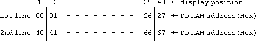
With the 40 character x 2 line display provided by the LM018L, when a display shift is performed the display will "wrap round". A Left shift will cause the character previously at display position 1 to "drop off" the left end and reappear at display position 40. A Right shift will cause the character previously at display position 40 to "drop off" the right end and reappear at display position 1.
Character Generator ROM (CG ROM)
The Character Generator ROM generates 5 x 7 dot or
5 x 10 dot character patterns from 8-bit character
codes. It contains 192 5 x 7 dot character patterns and
192 5 x 10 dot character patterns.
Character Generator RAM (CG RAM)
The Character Generator RAM is RAM with which the user can
redefine character patterns in software. With 5 x 7
dots, 8 user-defined character patterns can be stored and with
5 x 10 dots, 4 user-defined character patterns can be
stored.
| Instruction | CODE | D E S C R I P T I O N | Typical Execution Time | |||||||||
| RS | R/W | DB7 | DB6 | DB5 | DB4 | DB3 | DB2 | DB1 | DB0 | |||
| Clear Display |
0 | 0 | 0 | 0 | 0 | 0 | 0 | 0 | 0 | 1 | Clears display and returs the cursor to home position (address 0) Sets I/D= 1 of Entry Mode | 1.64µs |
| Return home | 0 | 0 | 0 | 0 | 0 | 0 | 0 | 0 | 1 | * | Return the cursor to the home position (Address 0). Also returns the display being shifted to the original position. DD RAM contents remain unchanged. Set DD RAM address to zero | 1.64µs |
| Entry mode set | 0 | 0 | 0 | 0 | 0 | 0 | 0 | 1 | I/D | S | Set the Cursor move direction and specifies or not to shift the display. These operations are performed during data write and read of DD RAM/CG RAM FOR NORMAL OPERATION SET S TO 0 | 40µs |
| Display on off control | 0 | 0 | 0 | 0 | 0 | 0 | 1 | D | C | B | Sets ON/OFF all display (D), cursor on/off (C), and blink of cursor position character(B) | 40µs |
| Cursor or Display shift | 0 | 0 | 0 | 0 | 0 | 1 | S/C | R/L | * | * | moves the cursor and shifts the display without changing DD RAM contents | 40µs |
| Function Set | 0 | 0 | 0 | 0 | 1 | DL | N | F | * | * | Sets interface data length(DL) number of display lines(N) and character font(F) | 40µs |
| Set the CG RAM address | 0 | 0 | 0 | 1 | MSB ACG | LSB | Set the CG RAM address. CG RAM data is sent and received after this setting. | 40µs | ||||
| Set the DD RAM address | 0 | 0 | 1 | MSB ADD | LSB | Set the DD RAM address. DD RAM data is sent and received after this setting. | 40µs | |||||
| Read bussy flag & address | 0 | 1 | BF | MSB AC | LSB | Reads Busy(BF) indicating internal operation is being performed and reads address counter contents. | 40µs | |||||
| Write data to CG or DD RAM | 1 | 0 | MSB | LSB | Writes data into DD RAM of CG RAM | 40µs | ||||||
| Read Data from CG or DD RAM | 1 | 1 | MSB ACG | LSB | Reads data into DD RAM of CG RAM | 40µs | ||||||
| S=1 | Accompanies display shift when data is written, For normal operations, set to 0 | DD RAM | Display Data RAM |
| I/D=1 | Increment DL=1 : 8 bits | CG RAM | Character Generator RAM |
| I/D=0 | Decrement DL=0 : 4 bits | ACG | CG RAM address |
| S/C=1 | Display Shift N =1 : 2(1) line | ADD | DD RAM address components to cursor address |
| S/C=0 | Cursor Move N =0 : 1 line | AC | Address count used for both DD and CG RAM address |
| R/L=1 | Shift to the right F=1 :5 x 10 dots | B | 1=ON 0=OFF(Blinking Cursor) |
| R/L=1 | Shift to the left f=0 : 5 x 7 dots | C | 1=ON 0=OFF(Cursor) |
| BF=1 | Internally operating | D | 1=ON 0=OFF(Display) |
| BF=0 | Can accept this instruction | * Don't care |
RS  R/W DB7 DB6 DB5 DB4 DB3 DB2 DB1 DB0
=== === === === === === === === === ===
 0   0   0   0   0   0   0   0   0   1
Clears all display and returns the cursor to the home position (Address 0).
Details
Writes space code "20" (Hexadecimal) (character pattern
for character code "20" must be blank pattern) into all
DD RAM addresses. Sets DD RAM address to 0 in the address
counter. Returns display to its original status if it was
shifted. In other words, the display disappears and the cursor or
blink go to the left edge of the display (the first line if 2
lines are displayed). Set I/D = 1 (Increment Mode) of Entry mode.
S of Entry Mode doesn't change.
Execution Time = 82µs-1.64ms / 120µs-4.9ms
RS  R/W DB7 DB6 DB5 DB4 DB3 DB2 DB1 DB0
 0   0   0   0   0   0   0   0   1   *
Returns the cursor to the home position (Address 0). Also returns the display being shifted to the original position. DD RAM contents remain unchanged.
Details
Sets the DD RAM address to 0 in the address counter. Returns the
display to its original status if it was shifted. DD RAM contents
do not change. The cursor or blink go to the left edge of the
display (the first line if 2 lines are displayed).
Execution Time = 40µs-1.6ms / 120µs-4.8ms
RS  R/W DB7 DB6 DB5 DB4 DB3 DB2 DB1 DB0
=== === === === === === === === === ===
 0   0   0   0   0   0   0   1  I/D  S
Sets the cursor move direction and specifies or not to shift the display. These operations are performed during data read and write.
Details
I/D: Increments (I/D = 1) or Decrements (I/D = 0) the DD RAM
address by 1 when a character code is written into or read from
the DD RAM. The cursor or blink moves to the right when
incremented by 1 and to the left when decremented by 1. The same
applies to writing to and reading from the CG RAM.
S: Shifts the entire display either to the right or to the left when S is 1; to the left when I/D = 1 and to the right when I/D = 0. Thus it looks as if the cursor stands still and the display moves.
Execution Time = 40µs / 120µs
RS  R/W DB7 DB6 DB5 DB4 DB3 DB2 DB1 DB0
=== === === === === === === === === ===
 0   0   0   0   0   0   1   D   C   B
Sets ON/OFF display, cursor and cursor position character (underscore) blink
Details
D: The display is ON when D = 1 and OFF when D = 0.
When off due to D = 0, display data remains in the DD RAM. It can
be displayed immediately by setting D = 1.
C: The cursor displays when C = 1 and does not
display when C = 0.
Even if the cursor disappears, the function of I/D, etc. does not
change during display data write.
The cursor is displayed using 5 dots in the 8th line when the 5 x
7 dot character font is selected and 5 dots in the 11th line when
the 5 x 10 dot character font is selected.
B: The character indicated by the cursor blinks
when B = 1.
The blink is displayed by switching between all blank dots and
display characters at 409.6 ms interval.
Execution Time = 40µs / 120µs
RS  R/W DB7 DB6 DB5 DB4 DB3 DB2 DB1 DB0
=== === === === === === === === === ===
 0   0   0   0   0   1  S/C R/L  *   *
Moves the cursor and shifts the display without changing DD RAM contents
Details
Shifts cursor position or display to the right or left without
writing or reading display data. This function is used to correct
or search for the display. In a 2-line display, the cursor moves
to the 2nd line when it passes the 40th digit of the 1st line.
Notice that the 1st and 2nd line displays will shift at the same
time. When the displayed data is shifted repeatedly each line
only moves horizontally. The 2nd line display does not shift into
the 1st line position.
S/C R/L
=== ===
 0   0   Shifts the cursor position to the left
         (Address Counter is decremented by 1)
 0   1   Shifts the cursor position to the right
         (Address Counter is incremented by 1)
 1   0   Shifts the entire display to the left
         The cursor follows the display shift
 1   1   Shifts the entire display to the right
         The cursor follows the display shift
Execution Time = 40µs / 120µs
RS  R/W DB7 DB6 DB5 DB4 DB3 DB2 DB1 DB0
=== === === === === === === === === ===
 0   0   0   0   1   DL  N   F   *   *
Sets interface data length (DL), number of display lines (N) and character font (F)
Details
DL: Sets interface data length
Data is sent or received in 8 bit lengths (DB7-DB0) when DL = 1
Data is sent or received in 4 bit lengths (DB7-DB4) when DL = 0
When the 4 bit length is selected, data must be sent or received twice.
N: Sets number of display lines
F: Sets character font
Note
Perform the function at the start of the program before executing
any instructions (except "Busy flag/address read").
From this point, the function set instruction cannot be executed
unless the interface data length is changed.
    display Character  Duty
N F  lines    Font    Factor Remarks
=== ======= ========= ====== =======
0 0    1    5x 7 dots  1/8    -
0 1    1    5x10 dots  1/11   -
1 *    2    5x 7 dots  1/16  Cannot display 2 lines with
                             5x10 dot character font
Execution Time = 40µs / 120µs
RS  R/W DB7 DB6 DB5 DB4 DB3 DB2 DB1 DB0
=== === === === === === === === === ===
 0   0   0   1   A   A   A   A   A   A
Sets the CG RAM address. CG RAM data is sent after this setting
Details
Sets the CG RAM address into the address counter in binary
AAAAAA. Data is then written to or read from the MPU for the CG
RAM.
Execution Time = 40µs / 120µs
RS  R/W DB7 DB6 DB5 DB4 DB3 DB2 DB1 DB0
=== === === === === === === === === ===
 0   0   1   A   A   A   A   A   A   A
Sets the DD RAM address. DD RAM data is sent after this setting
Details
Sets the DD RAM address into the address counter in binary
AAAAAAA. Data is then written to or read from the MPU for the DD
RAM.
However
when N = 0 (1 line display)
AAAAAAA is "00" - "4F" (Hex)
when N = 1 (2 line display)
AAAAAAA is "00" -
"27" (Hex) for the first line and
AAAAAAA is "40" - "67" (Hex) for the second line.
Execution Time = 40µs / 120µs
RS  R/W DB7 DB6 DB5 DB4 DB3 DB2 DB1 DB0
=== === === === === === === === === ===
 0   1   BF  A   A   A   A   A   A   A
Reads Busy flag (BF) indicating internal operation is being performed and reads address counter contents
Details
Reads the busy flag (BF) that indicates the system is now
internally executing a previously received instruction. BF = 1
indicates that internal operation is in progress. The next
instruction will not be accepted until BF is set to
"0". Check the BF status before the next wire
operation.
At the same time, the value of the address counter expressed in AAAAAAA is read out. The address counter is used by both CG and DD RAM addresses. Its current use is determined by the previous instruction.
Execution Time = 1µs
RS  R/W DB7 DB6 DB5 DB4 DB3 DB2 DB1 DB0
=== === === === === === === === === ===
 1   0   D   D   D   D   D   D   D   D
Writes data into DD RAM or CG RAM
Details
Writes binary 8 bit data DDDDDDDD to the CG or the DD RAM.
Whether the CG or DD RAM is to be written is determined by the
previous specification of CG RAM or DD RAM address setting. After
the write, the address is automatically incremented or
decremented by 1 according to entry mode. The entry mode also
determines display shift.
Execution Time = 40µs / 120µs
RS  R/W DB7 DB6 DB5 DB4 DB3 DB2 DB1 DB0
=== === === === === === === === === ===
 1   1   D   D   D   D   D   D   D   D
Reads data from DD RAM or CG RAM.
Details
Reads binary DDDDDDDD from the CG or DD RAM. The previous
designation determines whether the CG or DD RAM is to be read.
Before entering the read instruction, you must execute either the
CG RAM or DD RAM address set instruction. If you don't, the first
read data will be invalidated. When serially executing the
"read" instruction, the next address data is normally
read from the second read. The "address set"
instruction need not be executed just before the "read"
instruction when shifting the cursor by cursor shift instruction
(when reading out DD RAM). The cursor shift instruction operation
is the same as that of the DD RAM's address set instruction.
After a read, the entry mode automatically increases or decreases the address by 1. However, display shift is not executed no matter what the entry mode is.
Note:
The address counter (AC) is automatically incremented or
decremented by 1 after "write" instructions to either
CG RAM or DD RAM. RAM data selected by the AC cannot them be read
out even if "read" instructions are executed. The
conditions for correct data read out are: execute either the
address set instruction or cursor shift instruction (only with DD
RAM), just before reading out execute the "read"
instruction from the second time the "read" instruction
is serial.
Execution Time = 40µs / 120µs
Initialising by internal reset circuit
The HD44780 automatically initialises (resets) when power is turned on using the internal reset circuit. The following instructions are executed in initialisation. The busy flag (BF) is kept in busy state until initialisation ends. The busy state (BF=1) is 10ms after Vcc rises to 4.5volts.
1. Display clear

2. Function set ..... DL = 1: 8 bit interface
                       N = 0: 1 line display
                       F = 0: 5 x 7 dot character font

3. Display ON/OFF ...  D = 0: Display OFF
                       C = 0: Cursor OFF
                       B = 0: Blink OFF

4. Entry mode set .. I/D = 1: +1 (increment)
                       S = 0: No shift

5. Write DD RAM
   When the rise time of power supply (0.2 -> 4.5) is out
   of the range 0.1ms - 10ms, or when the low level width
   of power OFF (less than 0.2) is less than 1ms, the
   internal reset circuit will not operate normally.
   In this case, initialisation will not be performed
   normally. Initialise by instruction, as detailed below.
If the power supply conditions for correctly operating the internal reset circuit are not met, initialisation by instruction is required.
Initialising by instruction
When interface is 8-bits wide
              [Power ON]

       [  Wait more than 15ms  ]
       [after Vdd rises to 4.5v]

RS  R/W DB7 DB6 DB5 DB4 DB3 DB2 DB1 DB0  Can't check BF before this instruction
 0   0   0   0   1   1   *   *   *   *   Function set (8-bit interface)

        [Wait more than 4.1ms]

RS  R/W DB7 DB6 DB5 DB4 DB3 DB2 DB1 DB0  Can't check BF before this instruction
 0   0   0   0   1   1   *   *   *   *   Function set (8-bit interface)

        [Wait more than 100us]

RS  R/W DB7 DB6 DB5 DB4 DB3 DB2 DB1 DB0  Can't check BF before this instruction
 0   0   0   0   1   1   *   *   *   *   Function set (8-bit interface)

                                         BF can be checked after the following
                                         instructions. When BF is not checked,
                                         the waiting time between instructions
                                         is longer than the execution time.
                                         (See Instruction set)

RS  R/W DB7 DB6 DB5 DB4 DB3 DB2 DB1 DB0
 0   0   0   0   1   1   N   F   *   *   Function set  [8-bit Interface      ]
                                                       [Specify display lines]
RS  R/W DB7 DB6 DB5 DB4 DB3 DB2 DB1 DB0                [and character font   ]
 0   0   0   0   0   0   1   0   0   0   Display OFF    These cannot be
                                                        changed afterwards
RS  R/W DB7 DB6 DB5 DB4 DB3 DB2 DB1 DB0
 0   0   0   0   0   0   0   0   0   1   Display ON

RS  R/W DB7 DB6 DB5 DB4 DB3 DB2 DB1 DB0
 0   0   0   0   0   0   0   1  I/D  S   entry mode set

        [end of initialisation]
When interface is 4-bits wide
        [Power ON]

[  Wait more than 15ms  ]
[after Vdd rises to 4.5v]

RS  R/W DB7 DB6 DB5 DB4  Can't check BF before this instruction
 0   0   0   0   1   1   Function set (8-bit interface)

    [Wait more than]
    [     4.1ms    ]

RS  R/W DB7 DB6 DB5 DB4  Can't check BF before this instruction
 0   0   0   0   1   1   Function set (8-bit interface)

    [Wait more than]
    [     100us    ]

RS  R/W DB7 DB6 DB5 DB4  Can't check BF before this instruction
 0   0   0   0   1   1   Function set (8-bit interface)

                         BF can be checked after the following
                         instructions. When BF is not checked,
                         the waiting time between instructions
                         is longer than the execution time.
                         (See Instruction set)

RS  R/W DB7 DB6 DB5 DB4
 0   0   0   0   1   0   Function set (to 4-bit interface)

RS  R/W DB7 DB6 DB5 DB4
 0   0   0   0   1   0
 0   0   N   F   *   *   Function set  [4-bit Interface      ]
                                       [Specify display lines]
RS  R/W DB7 DB6 DB5 DB4                [and character font   ]
 0   0   0   0   0   0                  These cannot be
 0   0   1   0   0   0   Display OFF    changed afterwards

RS  R/W DB7 DB6 DB5 DB4
 0   0   0   0   0   0
 0   0   0   0   0   1   Display ON

RS  R/W DB7 DB6 DB5 DB4
 0   0   0   0   0   0
 0   0   0   1  I/D  S   entry mode set

[end of initialisation]